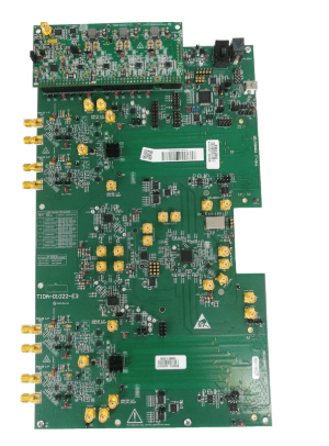
This reference design serves several applications, including oscilloscopes (DSOs), data acquisition (DAQ) systems, and electronic warfare, where high-speed signal acquisition is critical.

This reference design TIDA-010128 by Texas Instruments (TI) outlines a high-performance 20.8 GSPS (Giga samples per second) sampling system using RF-sampling analog-to-digital converters (ADCs) arranged in a time-interleaved configuration. Time interleaving is a proven method to achieve higher sampling rates by using multiple ADCs to sample at equally spaced intervals, combining their outputs for a higher overall sampling rate. However, the interleaving method introduces challenges in matching each ADC’s offset, gain, and sampling time mismatch, which are crucial for maintaining optimal performance. The complexity of achieving accurate interleaving increases as the sampling clock speed rises, requiring precise synchronization between ADCs to ensure superior spurious-free dynamic range (SFDR) and effective number of bits (ENOB).
To address these challenges, this reference design leverages the noiseless aperture delay adjustment feature of the ADC12DJ5200RF device. This feature allows for 19 femtosecond (fs) phase control steps, making the 20.8 GSPS interleaving feasible by minimizing timing mismatches between ADCs. The design also incorporates a low-noise JESD204B clock generator, which uses the LMK04828 and LMX2594 devices, ensuring high system performance while meeting the 12-bit resolution requirement. The reference design is equipped with several key features, including 20.8 GSPS time-interleaved, 12-bit, RF-sampling ADCs, a 6-GHz analog front end, fine sample clock phase adjustment with 19 fs resolution, and phase synchronization of multiple ADCs. It also includes a companion power reference design, achieving over 85% efficiency with a 12-V input, and supports JESD204B with up to 32 lanes at data rates up to 12.8 Gbps per lane.
The design features an FMC+ connector, making it compatible with TI’s TSW14J57EVM capture card, which is ideal for high-speed data acquisition systems. The time-interleaving approach demonstrated here addresses the key design challenges of reducing timing errors and optimizing system performance, particularly in terms of signal-to-noise ratio (SNR), SFDR, and ENOB. The hardware platform provides a flexible clocking solution that enables designers to validate system performance with a range of clocking source options. The onboard LMX2594 clock synthesizer offers excellent phase noise characteristics at high frequencies, ensuring reliable clocking for the ADCs. The ADC12DJ5200RF is a high-speed RF-sampling ADC capable of directly sampling input frequencies from DC to over 10 GHz, with a sampling rate of up to 5.2 GSPS in dual-channel mode and 10.4 GSPS in single-channel mode.
The LMK0482x clock family provides the highest performance clock conditioning with JESD204B support, and the LMX2594 PLL synthesizer delivers a wide frequency range without the need for an internal doubler, making it an ideal choice for this high-performance system. TI has tested this reference design. It comes with a bill of materials (BOM), schematics, assembly drawing, printed circuit board (PCB) layout, and more. The company’s website has additional data about the reference design. To read more about this reference design, click here.


