

The testing method checks micro-LED wafers without damage. It uses soft probes and tools to improve yield, lower costs, and speed up inspection.

Scientists at Tianjin University have created a new nondestructive testing method for micro-LED wafers, using a unique “soft-touch” technique to address a key industry problem.
Micro-LEDs are seen as a core technology for future high-end displays. To maintain quality and reduce repair costs, manufacturers must achieve very high yields during wafer production. However, reliably testing these wafers without damaging them has long been a technical barrier. This new approach offers a possible path forward.

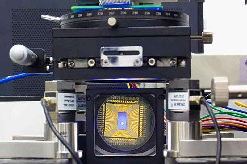
The research team has developed a flexible three-dimensional probe array that adapts to the microscopic surface of micro-LED wafers, applying minimal pressure—around 0.9 MPa—enabling electrical testing without scratching or damaging the wafer. This soft-contact method supports high-throughput testing while protecting delicate surfaces.
The contact pressure of these flexible probes is just one-ten-thousandth that of traditional rigid probes. This not only preserves the wafer surface but also extends the probes’ service life. Even after one million contact cycles, the probes remain in original condition.
To complement the probe array, the team designed a specialized measurement system that works in tandem with the flexible probes. Together, they offer a practical solution for process monitoring and yield screening in micro-LED production.
This advancement addresses a long-standing gap in micro-LED electroluminescence testing and lays the groundwork for broader use in wafer inspection and biophotonics.
The technology is now moving toward commercialization at a local innovation park. It aims to deliver a scalable, low-cost, and nondestructive testing platform for the expanding micro-LED sector, with potential to impact other areas of flexible electronics as well.