

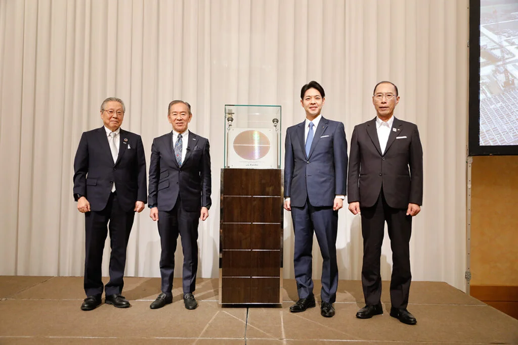
Facing high stakes, yet higher ambitions, Japan’s Rapidus presents the chip world with its first 2nm prototype chip. Will this big bet be able to compete with the giants like TSMC?
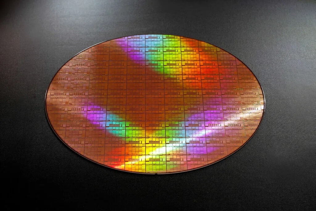
On July 18, at a press event in Chitose, Hokkaido, Japanese firm Rapidus Corporation confirmed that it had successfully validated the country’s first prototype chip built on cutting-edge 2-nanometre (nm) Gate-All-Around (GAA) transistor technology.
This breakthrough marks a vital step for Japan in decades to re-enter the elite tier of advanced semiconductor manufacturing; an industry it once led, but long ceded to rivals like Taiwan’s Taiwan Semiconductor Manufacturing Company (TSMC) and South Korea’s Samsung. Backed by government support and global partnerships, the prototype, perhaps, signals a strategy to close the technology gap and reduce dependency on foreign fabs amid escalating geopolitical risks.
Rapidus said it plans to offer chip design kits to customers by early 2026, with mass production targeted for 2027, making it a potential fourth global player in the race to commercialise 2nm chips.
A tech gamble with national stakes
Founded in August 2022, Rapidus was born out of Japan’s concerns over the concentration of advanced semiconductor production in Taiwan. According to a retrospective in Japan Forward, the idea of building domestic 2nm chips originated from a proposal made by IBM to Tetsuro Higashi, former head of Tokyo Electron and now chairman of Rapidus. IBM, having developed 2nm technology in 2021, sought a trusted international partner to scale it.
Following internal evaluations and national consultations, Rapidus was launched as a public–private partnership, with founding investments and backing from Toyota, Sony, NTT, NEC, SoftBank, and MUFG, under the leadership of Japan’s Ministry of Economy, Trade and Industry (METI). The project has since received over ¥1.7 trillion (approx. US$11.6 billion) in public funding, with an additional ¥100 billion planned for later in 2025 under new legislation.
The 2nm chips use GAA nanosheet transistors, an evolution from FinFET technology, offering improved power efficiency and greater control at reduced sizes. According to a report by Bloomberg, the company has recently begun fabricating wafers using Extreme Ultraviolet (EUV) lithography systems supplied by ASML, one of the world’s most advanced semiconductor manufacturing platforms.
This high-resolution process not only improves patterning precision but also creates a valuable feedback loop that supports the training of AI models to predict and optimise wafer yield, an essential factor in next-generation chip production. Rapidus stated that it is among the first to pursue full-scale single-wafer processing, a key pillar of its proprietary Rapid and Unified Manufacturing Service (RUMS) model.
At the heart of this model is EUV lithography, critical for producing 2nm GAA structures. In December 2024, Rapidus became the first Japanese company to install ASML’s cutting-edge EUV tools. By April 1, 2025, just three months later, it had already completed successful EUV exposure.
President Atsuyoshi Koike reportedly stated that the company achieved this technological breakthrough at an unprecedented pace. He acknowledged that while the roadmap to mass production remains challenging, particularly in improving yield and reliability, the company is on track to support customer chip prototyping by March 2026.
Unique manufacturing model
Rather than mimicking the high-volume fabs of TSMC or Samsung, Rapidus has adopted a distinctive single-wafer processing approach. As described by Tom’s Hardware, this method allows wafers to be handled individually instead of in batches, enabling real-time feedback and data collection during fabrication. While this comes with trade-offs in throughput and cost, it provides engineers with faster insights to correct defects and optimise performance, critical in prototype phases.
Koike has said previously that this model enables the company to refine designs more quickly and respond flexibly to customer-specific needs, particularly in fields like artificial intelligence (AI), autonomous vehicles, and edge computing: areas where Japan seeks to regain technological leadership.
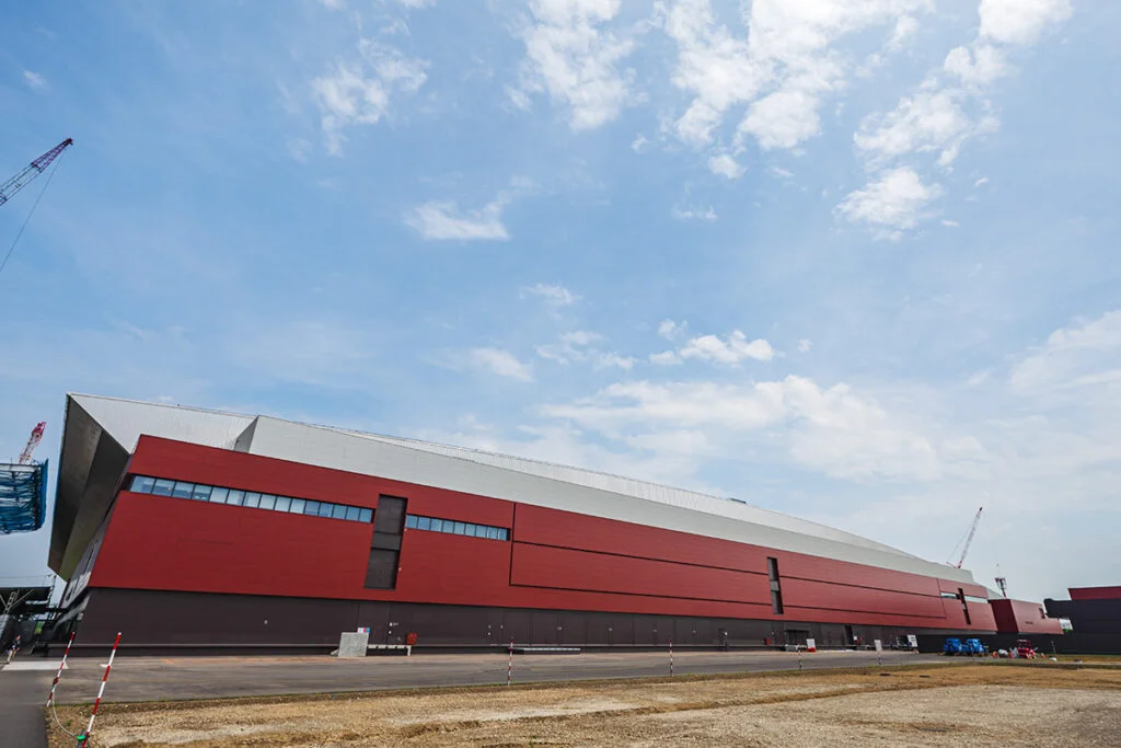
Chitose’s IIM-1 fab, a landmark
The prototype was developed at IIM-1, Rapidus’s state-of-the-art semiconductor facility in Chitose City, Hokkaido, where construction began in September 2023. As of mid-2025, the factory is approximately 80% complete, with more than 200 tools already installed, including the EUV equipment that enabled 2nm chip printing. The cleanroom was activated in April 2025, when pilot production officially began in May.
Local officials such as Governor Naomichi Suzuki and Mayor Ryuichi Yokota of Chitose have been publicly supportive.
Meanwhile, Japan’s declining chip industry in the past decades had not completely eroded its engineering base. Rapidus drew on this legacy by sending around 150 Japanese engineers to IBM’s research facilities in Albany, New York. Around 70 of them have since returned, applying their newly acquired knowledge to Rapidus’s pilot line in Chitose. This strategy not only expedited skill transfer but also anchored next-generation semiconductor expertise back in Japan.
The global competitive edge
If successful, Rapidus would become the fourth entity worldwide to reach 2nm production readiness, after TSMC, Samsung, and Intel. According to Reuters, the company has already engaged in exploratory discussions with potential customers, including Apple, Google, Amazon, Microsoft, and Meta, though no confirmed contracts have yet been announced.
Former Intel CEO Pat Gelsinger had previously noted that Rapidus’s best strategy would be to avoid competing directly with the likes of TSMC and instead carve out a unique position in the custom AI and high-performance logic segment.
Risks and rewards
The stakes for Japan are high. Experts have warned that if Rapidus fails, Japan’s equipment and material suppliers, which are still globally competitive, may be forced to relocate. They have argued that this would undermine the nation’s broader industrial base, including sectors such as automotive and robotics that depend on advanced chips.
Yet, if successful, the Rapidus project could re-anchor Japan as a sovereign player in critical technologies. As the country looks beyond its ageing automotive sector for a new growth engine, semiconductors offer a compelling opportunity. The government’s investment, its engineering recalibration, and global partnerships have placed Japan back in the conversation, if not as a volume leader, then certainly as a strategic innovator.
As the first chips emerge from Hokkaido’s cleanrooms, the world will be watching to see if this ambitious experiment in industrial policy and innovation pays off.